Table of Content
It does make me wonder how it might be possible to modify other photoresist application methods to accommodate this process. I really like the laser printer based photoresist method since it’s so precise. On the other hand, you can use homemade PCBs for prototypes and replace defective PCBs that you can't find on the market. In this case, ordering 1000 PCBs for fixing your Grandpa's old radio doesn't make sense. In addition, the copper foil is much thinner than the layer of copper you use in DIY projects. The thickness of a 2 layer PCB is typically around 3.2 mm, but can range from 2.8 mm to 4.0 mm.
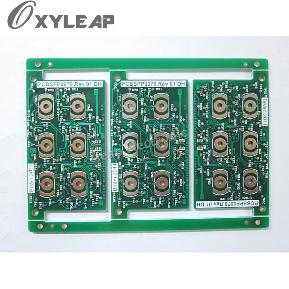
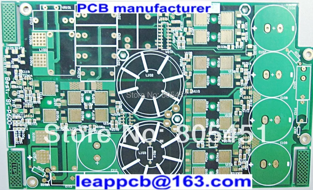
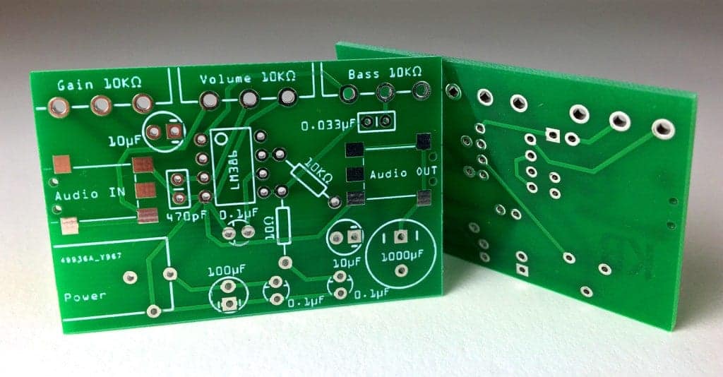
They can be single or double-sided and may have multiple layers. Most standard PCB are assembled using surface mount technology , though through-hole components are also used in some cases. Standard PCBs typically have a solder mask and protective coating to prevent shorts and help protect the components from damage. The most common type of finish is hot air soldering level , though other finishes, such as immersion gold, are also used in some applications. A printed circuit board has pre-designed copper tracks on a conducting sheet. The pre-defined tracks reduce the wiring thereby reducing the faults arising due to lose connections.
Checking if the site connection is secure
The Fecl3 reacts with the unmasked copper and removes the unwanted copper from the PCB. Use pliers to take out the PCB and check if the entire unmasked area has been etched or not. In case it is not etched leave it for some more time in the solution. Put a white paper on the OHP sheet and start ironing.
There are rivets making this easier than short lengths of wire. At such sizes, one can press rivets by hand-force, without a machine. It is the need to store all of those toxic chemicals, use them, dispose of the waste and clean up the mess. Instead, I just push a button and a week later take delivery of a far better PCB than 99.9% of the hobbyists could make.
Step 6: Peeling The Paper
When you have fully etched the board, you can remove it using the pliers from the solution. The PCBs made in a factory have laser-precision accuracy. Factories manufacture PCBs in cleanrooms to avoid dust getting on the boards; that's why you shouldn't expect your homemade PCB to replace an Intel motherboard. Circuit by hand on PCB is limited to our artistic skills. Simple circuit can easily be made by this method but for complex pcb Iron on Glossy paper is best.
It's also a good space to add your soft furnishings. Think pillows and throws for an instant added coziness to the space. As well as art, small accessories that fill the room can stop the space from feeling too stark. Candles placed artfully on a shelf over the backsplash. Beautiful vases on display to colored glass bottles you might have kept - making a stylish taper candle holder.
Step 3: Preparation of the Single-sided Copper Board.
Even the time saving doesn’t buy you much if you have to order parts to be delivered anyway. I get a Chinese PCB delivery fast than a Mouser or Digikey order. Apply thinner to a piece of clothes and remove the remaining toner. Print the design on the photo/gloss paper and cut the design out of the article.
We've covered both methods mentioned earlier, so use either way that suits you. I am a responsible, intelligent and experienced business professional with an extensive background in the electronics industry. I have developed a PCB, when i plug the 12V dc power, the board producing shocks.
Step 1: Designing of the Circuit
Increasing the roughness of the copper to enhance the bond strength of the laminate is a critical step. In addition, this process Prevents separation between different layers of the substrate. Many manufacturers use special laser direct imaging equipment to image directly on the dry film. In addition, the process is more accurate and efficient. Therefore, you can use direct laser imaging to generate inner and outer layers .
Hold one end of it by the Towel and put the hot iron on the other end for about 10 seconds. Now, iron the photo paper all along using the tip and applying little pressure for about 5 to 15 mins. Put the board and photo paper arrangement on a clean wooden table and clothes with the back of the photo paper facing you. Align each copper sheet precisely & secure them together using 5 min epoxy glue. Let it dry for a couple of minutes and clean it using Acetone or any other cleaner. I have used the P-N-P Blue as well and it works well.
To make the board etch evenly, you can gently move the plastic box to and fro so that the etching solution reacts with exposed copper and form iron and copper chloride. After every 2-3 minutes check whether all copper is etched or not. You also need FeCl3 powder/solution , photo/glossy paper, a permanent black marker, a blade cutter, sandpaper, kitchen paper, and cotton wool.
Batch auto-routing-the designer will do the routes manually and set several design rules to guide the process. It is the work of the client to come up with the idea of what should go into the PCB as the designer will build the schematic depending on the idea. Every component that is to be used in the design has a symbol that is placed on the board to represent the component. Finding the material for this process is not for average people. Holes can be drilled using a drill either homemade or commercially available PCB drilling drills. Take a toothbrush and gently brush it off as shown below.
The heat applied by the electric iron causes the ink of the traces on the OHP sheet to stick on the copper plate exactly in the same way it is printed on the OHP sheet. This means that the copper sheet will now have the layout of the PCB printed on it. Allow the PCB plate to cool down and slowly remove the OHP sheet. Since it is manual process it may happen that the layout doesn’t comes properly on PCB or some of the tracks are broken in between. Use the permanent marker and complete the tracks properly. Surface treatmentis the last and final chemical process in the manufacture of multilayer printed circuit boards.


No comments:
Post a Comment